Carrier-SM-B79

Depending on the configuration and following revisions, the features of the board are subject to change. For detailed information on hardware specifications, please visit www.seco.com
This carrier board is contained in the development kit DEV-KIT- SMARC
How can I configure jumpers?
| Component | Description | Use | Default configuration (Fig.1) |
|---|---|---|---|
| CN64 | SER2 | Set no jumper for 120 ohm termination for A-B and Y-Z | |
| Set jumper 1-2 for 120 ohm termination for A-B only | |||
| Set jumper 2-3 for no 120 ohm terminations | Unplugged | ||
| CN63 | SER0 | Set no jumper for 120 ohm termination for A-B and Y-Z | |
| Set jumper 1-2 for 120 ohm termination for A-B only | |||
| Set jumper 2-3 for no 120 ohm terminations | Unplugged | ||
| CN24 | COM2 | Set no jumper for RS-485 | |
| Set jumper 1-2 for RS-422 | |||
| Set jumper 2-3 for RS-232 | Unplugged | ||
| CN23 | COM0 | Set no jumper for RS-485 | |
| Set jumper 1-2 for RS-422 | |||
| Set jumper 2-3 for RS-232 | Unplugged | ||
| CN78 | SMARC v2.1 | Set jumper 1-2 for SMARC V2.1 specs | |
| Set jumper 2-3 for SMARC V2.0 specs | 2-3 Plugged | ||
| JP7 | GPIO | ||
| JP12 | CAN0 | Set no jumper no termination | |
| Set jumper for 120 ohm termination | Plugged | ||
| JP13 | CAN1 | Set no jumper no termination | |
| Set jumper for 120 ohm termination | Plugged | ||
| CN67 | PCIE_SEL_AB, PCIE_SEL_CD | Set jumper 3-1 for PCIE A, B, C, D - X4 | |
| Set jumper 3-4 for PCIE A, B - X2, PCIE C - X1, PCIE D - M.2 (Modem) | |||
| Set jumper 3-5 for PCIE A - X1, PCIE B - M.2 (WiFi), PCIE C - X1, PCIE D - M.2 | |||
| (Modem) | 3-5 Plugged | ||
| CN75 | HDMI_DP1#_SEL | Set jumper 1-2 to select HDMI | |
| Set jumper 2-3 to select DP1 | 1-2 Plugged | ||
| CN76 | DP1_AUX_SEL | Set jumper 3-1 for fixed DDC selection (debug | |
| configuration) | |||
Set jumper 3-4 for adapter depending AUX/DDC selection (standard | |||
| configuration) | |||
| Set jumper 3-5 for fixed AUX selection (debug configuration) | 3-1 Plugged | ||
| CN62 | VIN_PWRBAD# | Set jumper 1-2 NO VIN_PWRBAD# control | |
| Set jumper 2-3 VIN_PWRBAD# is VSMARC_PG | 1-2 Plugged | ||
| JP14 | I2C EEPROM WP | Set no jumper to enable writes | |
| Set jumper 1-2 to disable writes | Unplugged | ||
| JP5 | SDIO_WP | Set no jumper to disable writes on SD Card | |
| Set jumper 1-2 to enable writes on SD Card | 1-2 Plugged | ||
| JP17 | |||
| JP18 | |||
| JP15 | W_DISABLE1/2#_E | ||
| Set no jumper for card enabled | |||
| Set jumper 1-2 for card disabled | Unplugged | ||
| JP16 | |||
| CN53 | SUS_S5 | Set jumper 1-2 for normal operation | |
| Set jumper 2-3 to force *_A voltages to be enabled | 1-2 Plugged | ||
| CN55 | FAN | Set jumper 1-2 for 12V FAN | |
| Set jumper 2-3 for 5V FAN | 1-2 Plugged | ||
| CN8 | VSMARC | Set jumper 1-2 for 3V | |
| Set jumper 3-4 for 3.3V | |||
| Set jumper 5-6 for 4.25V | |||
| Set jumper 7-8 for 5V | 1-2 Plugged | ||
| CN21 | VDD_BKLT1 | Set jumper 1-2 for 12V BKLT Power | |
| Set jumper 2-3 for 5V BKLT Power | 2-3 Plugged | ||
| CN20 | VDD_LCD1 | Set jumper 1-2 for 3.3V Panel Power | |
| Set jumper 2-3 for 5V Panel Power | 1-2 Plugged | ||
| CN19 | VDD_BKLT0 | Set jumper 1-2 for 12V BKLT Power | |
| Set jumper 2-3 for 5V BKLT Power | 2-3 Plugged | ||
| CN18 | VDD_LCD0 | Set jumper 1-2 for 3.3V Panel Power | |
| Set jumper 2-3 for 5V Panel Power | 1-2 Plugged |

Fig. 1: Description of possible jumpers configuration
How can I configure micro switches?
| Descrpition | Position | Use | Default configuration (Fig.2) |
|---|---|---|---|
| SW14 | Position 1-3 | ||
| TEST# | OFF for normal operation ON for test mode | OFF | |
| Position 2-4 | |||
| LID_BTN# | OFF for normal operation | ||
| ON for LIDBTN simulation | OFF | ||
| SW12 | Position 1-3 | ||
| BOOT_SEL0# | Fig.3 | OFF | |
| Position 2-4 | |||
| BOOT_SEL1# | Fig.3 | OFF | |
| SW13 | Position 1-3 | ||
| BOOT_SEL2# | Fig.3 | ON | |
| Position 2-4 | |||
| FORCE_RECOV# | Fig.3 | OFF | |
| SW6 | Position 1-3 | ||
| LVDS_eDP#_SEL | OFF for LVDS/DSI | ||
| ON for eDP | |||
| Position 2-4 | |||
| I2S_HDA#_SEL | OFF for I2S | ||
| ON for HDA | ON | ||
| SW7 | SER1_SEL | OFF for SER1 - Feature header | |
| ON for SER1 - USB microB (debug) | OFF |

Fig. 2: Description of possible switches configuration
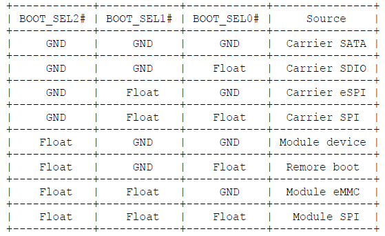
Fig. 3: Description of SW13 and SW14
What to connect and where?
Further information about placement and description of connectors are available here.